
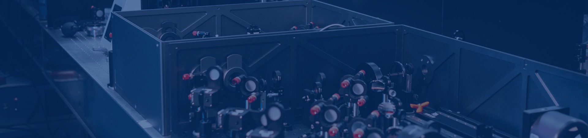

The Y300 Automatic Absorption Spectrometer for Semi-Insulating SiC Wafers is designed for production quality control of AR optical substrates. It integrates transmittance, reflectance, absorptance, refractive index, and haze measurements in one system, providing reliable data for evaluating the optical performance and consistency of optical-grade SiC wafers. Covering the near-ultraviolet to visible range of 370–800 nm, Y300 accommodates 6-, 8-, and 12-inch wafers and also supports other transparent materials, including glass, polymers, and fused silica.
Y300 uses a synchronized three-spectrometer architecture to acquire transmittance and reflectance data and calculate absorptance. Real-time reference compensation and wafer-by-wafer dynamic automatic calibration minimize the effects of light-source fluctuations and environmental drift, delivering measurement repeatability of less than 0.02%. Multi-point measurement and full-wafer imaging reveal spatial variations in optical properties, supporting material screening, process optimization, and outgoing quality inspection.
For continuous production, Y300 combines a non-contact automated wafer handling system with a horizontal sample stage, delivering a throughput of approximately 60 wafers per hour. It integrates with semiconductor automation lines and supports unattended operation around the clock. By combining highly repeatable optical characterization with automated inspection, Y300 helps manufacturers improve quality consistency and inspection efficiency for AR optical substrates.
Y300 uses a synchronized three-spectrometer architecture to acquire transmittance and reflectance data and calculate absorptance. Real-time reference compensation and wafer-by-wafer dynamic automatic calibration minimize the effects of light-source fluctuations and environmental drift, delivering measurement repeatability of less than 0.02%. Multi-point measurement and full-wafer imaging reveal spatial variations in optical properties, supporting material screening, process optimization, and outgoing quality inspection.
For continuous production, Y300 combines a non-contact automated wafer handling system with a horizontal sample stage, delivering a throughput of approximately 60 wafers per hour. It integrates with semiconductor automation lines and supports unattended operation around the clock. By combining highly repeatable optical characterization with automated inspection, Y300 helps manufacturers improve quality consistency and inspection efficiency for AR optical substrates.
Inquire

