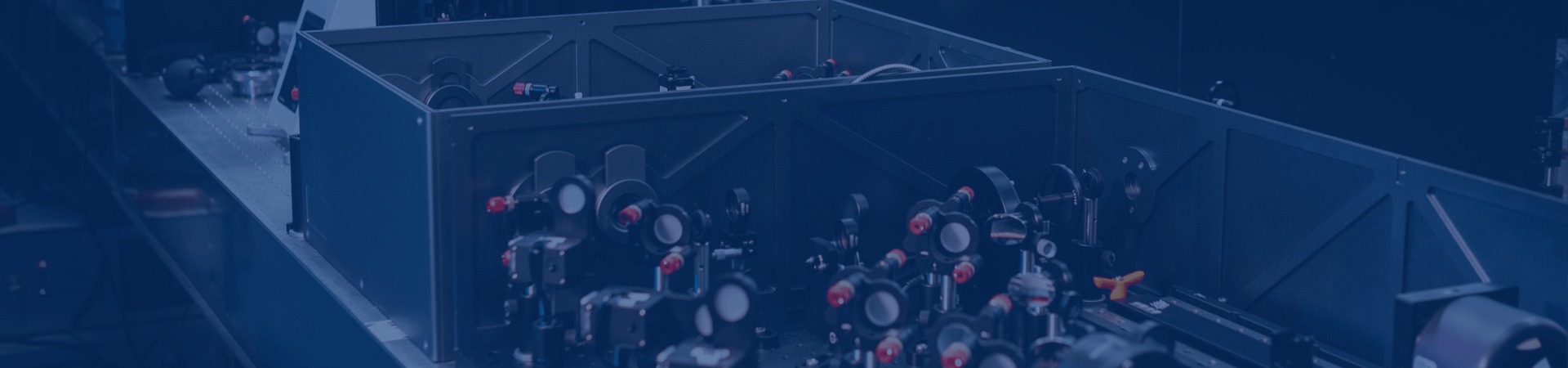

The DISPEC-9000 Fully Automated Non-destructive Optical Inspection System characterizes dislocation defects in N-type SiC substrate wafers. It combines defect identification, density analysis, and spatial mapping to support material quality control, production inspection, and process optimization.
The system supports inspection of both the Si-face and C-face and accommodates 6-, 8-, and 12-inch wafers. Inspection throughput is 4–5 wafers per hour for 6-inch wafers, 2–3 wafers per hour for 8-inch wafers, and 1 wafer per hour for 12-inch wafers. A single measurement simultaneously captures signals from threading edge dislocations (TEDs), threading screw dislocations (TSDs), and basal plane dislocations (BPDs). The system also supports detection of stacking faults (SFs), micropipes (MPs), carbon inclusions, heterocrystalline defects, and other defect types, enabling defect assessment across multiple substrate wafer sizes.
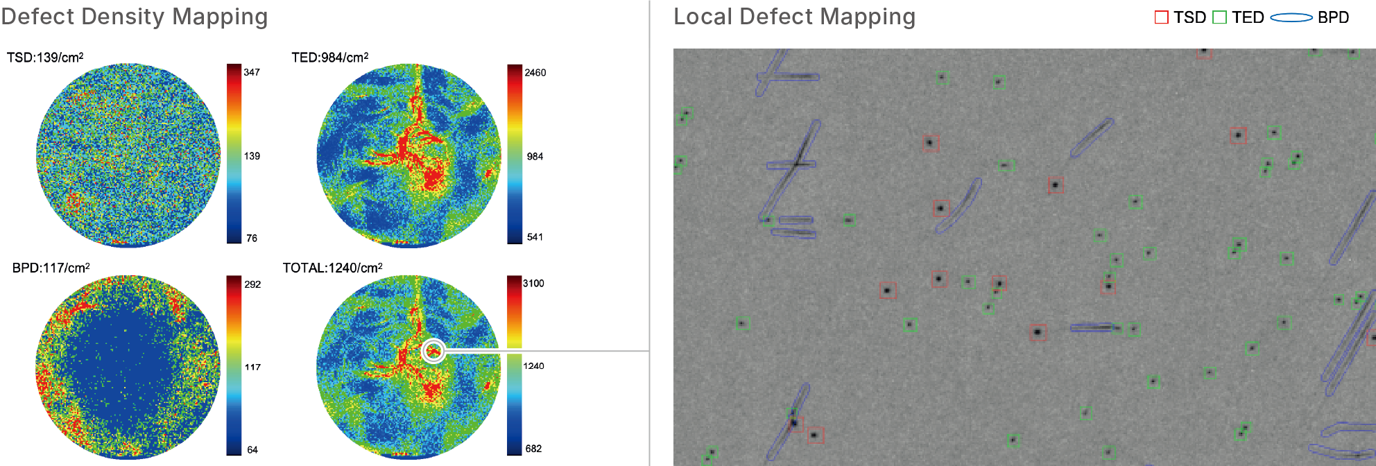
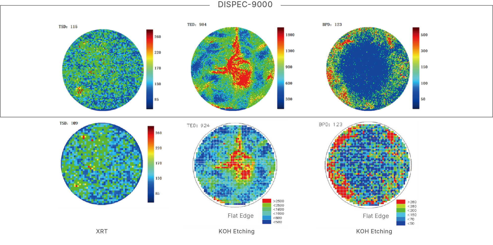
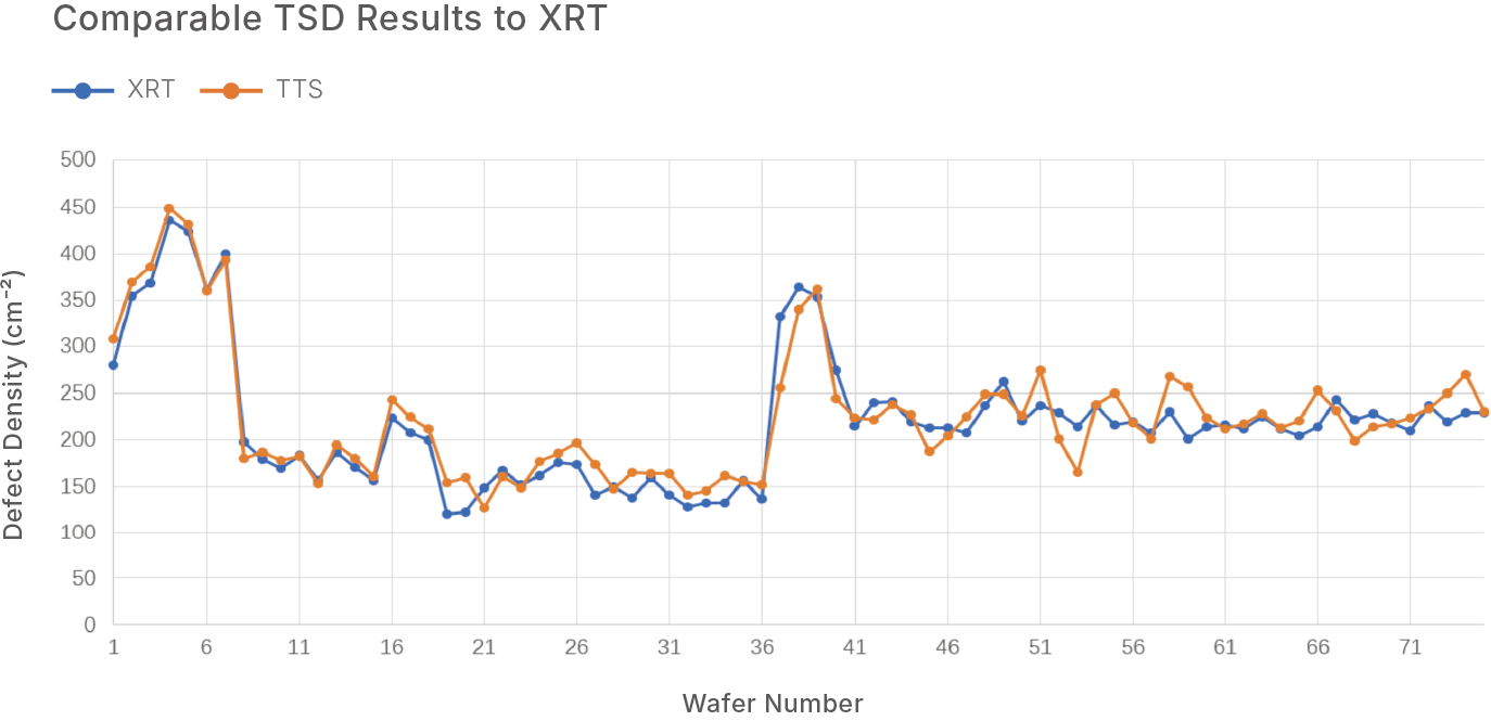
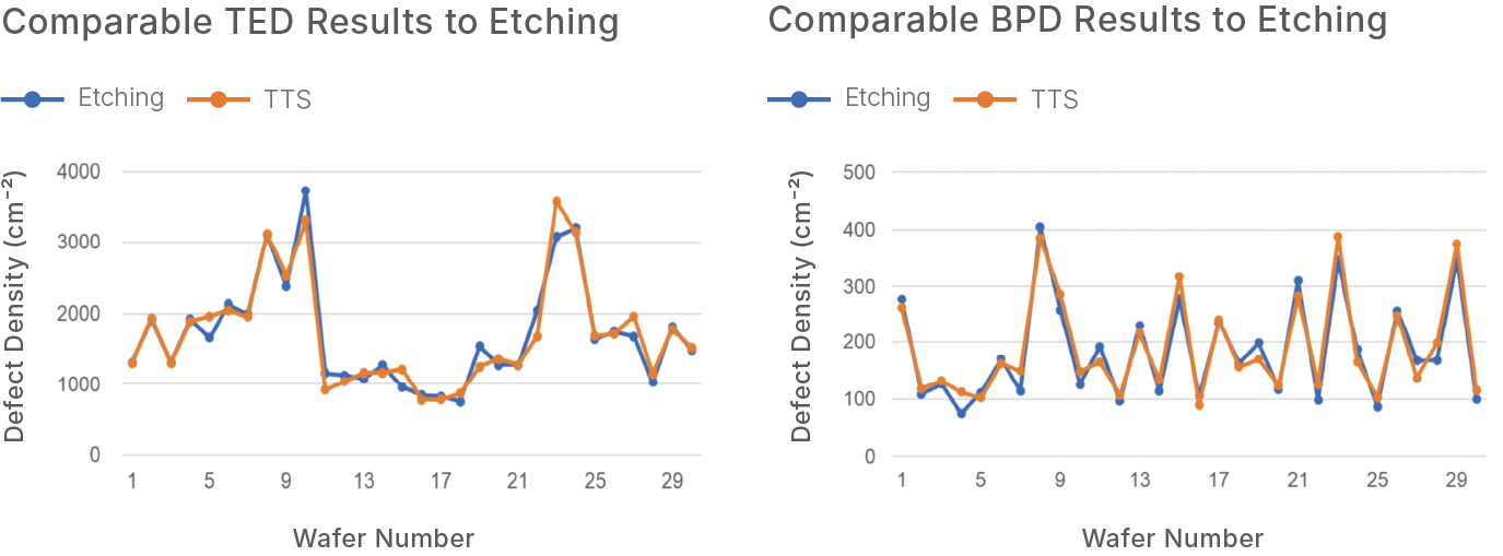
AI-assisted defect identification and density analysis, together with user-defined defect analysis, enable the system to produce optical images and defect density maps simultaneously, revealing defect features and their distribution across the wafer. Comparative testing shows close agreement with X-ray topography (XRT) for TSD detection and with KOH etching for TED and BPD detection. Repeated measurements on the same instrument and comparisons between instruments also demonstrate good repeatability and reproducibility.
The system supports inspection of both the Si-face and C-face and accommodates 6-, 8-, and 12-inch wafers. Inspection throughput is 4–5 wafers per hour for 6-inch wafers, 2–3 wafers per hour for 8-inch wafers, and 1 wafer per hour for 12-inch wafers. A single measurement simultaneously captures signals from threading edge dislocations (TEDs), threading screw dislocations (TSDs), and basal plane dislocations (BPDs). The system also supports detection of stacking faults (SFs), micropipes (MPs), carbon inclusions, heterocrystalline defects, and other defect types, enabling defect assessment across multiple substrate wafer sizes.
AI-assisted defect identification and density analysis, together with user-defined defect analysis, enable the system to produce optical images and defect density maps simultaneously, revealing defect features and their distribution across the wafer. Comparative testing shows close agreement with X-ray topography (XRT) for TSD detection and with KOH etching for TED and BPD detection. Repeated measurements on the same instrument and comparisons between instruments also demonstrate good repeatability and reproducibility.
Inquire