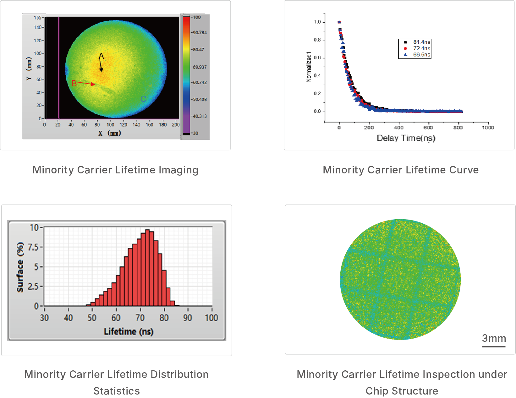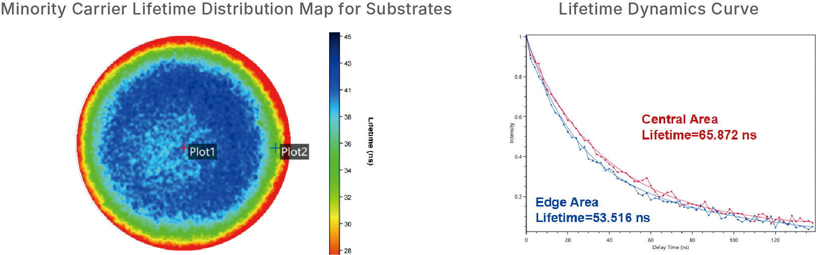

TAU-9000/9000HR High-Resolution SiC Wafer Minority Carrier Lifetime Imaging Tools uses time-resolved spectroscopic imaging to characterize SiC substrates and epitaxial wafers. It supports material qualification, production inspection, and R&D, providing measurement data for quality control, process optimization, and defect analysis.
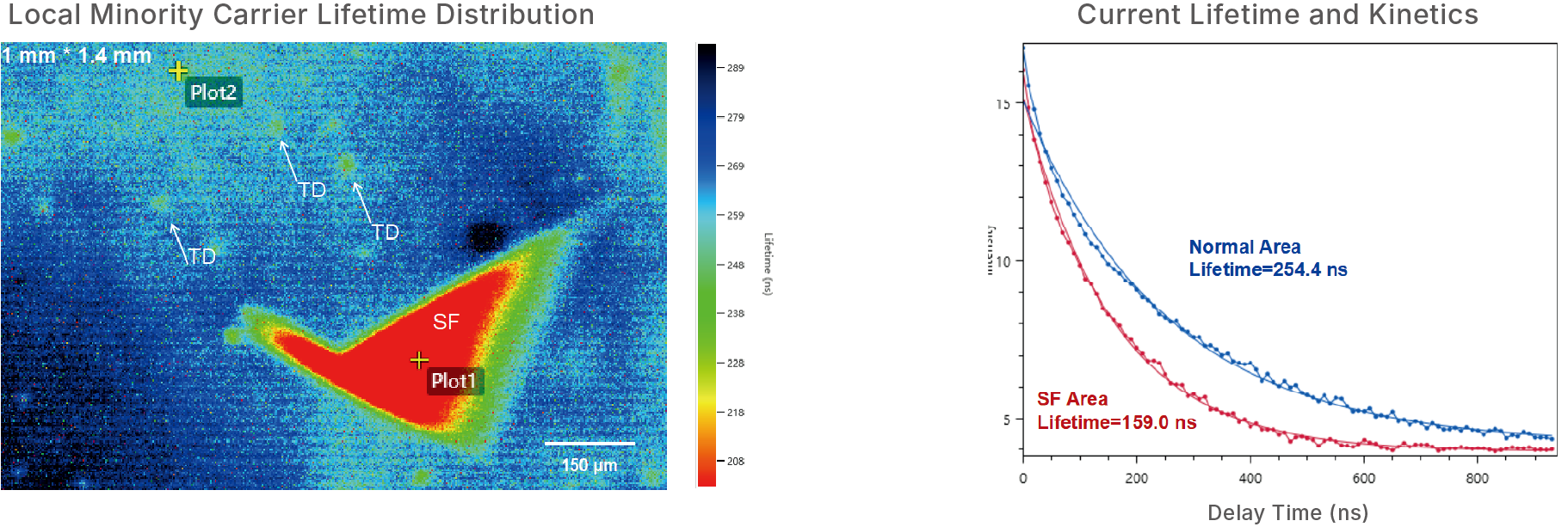
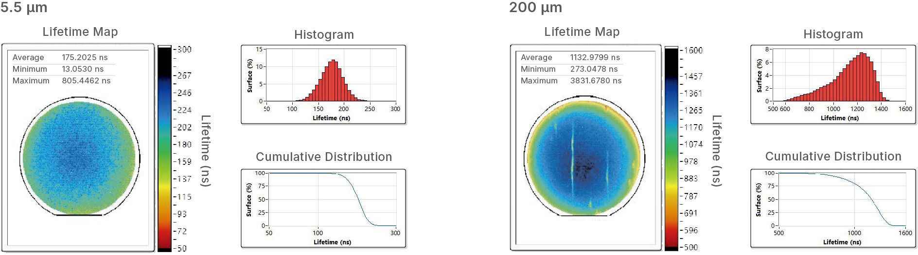
These tools support both full-wafer mapping and localized microscopic imaging. In full-wafer mode, it achieves a spatial resolution of 100 μm to characterize minority carrier lifetime distributions and uniformity. It accommodates 6-, 8-, and 12-inch wafers, with measurement times of less than 10 minutes per 6-inch wafer. In microscopic mode, spatial resolution reaches 0.9 μm, enabling visualization of lifetime variations associated with threading dislocations and stacking faults. A temporal resolution of <2 ns enables characterization of both short-lifetime substrates and epitaxial layers.
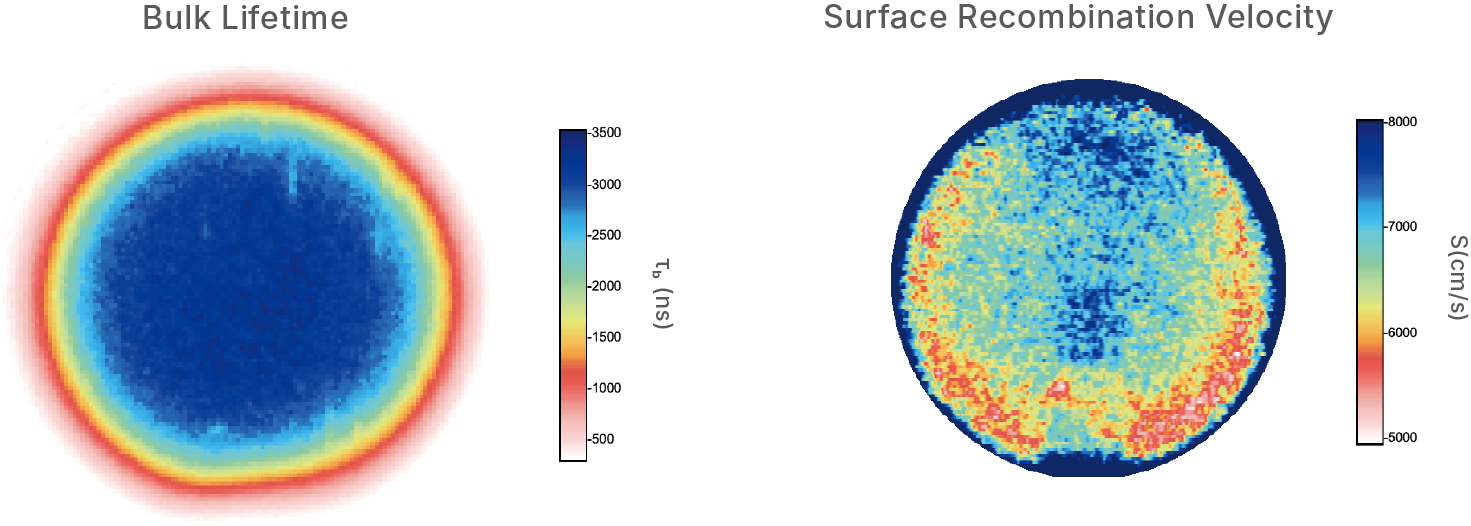
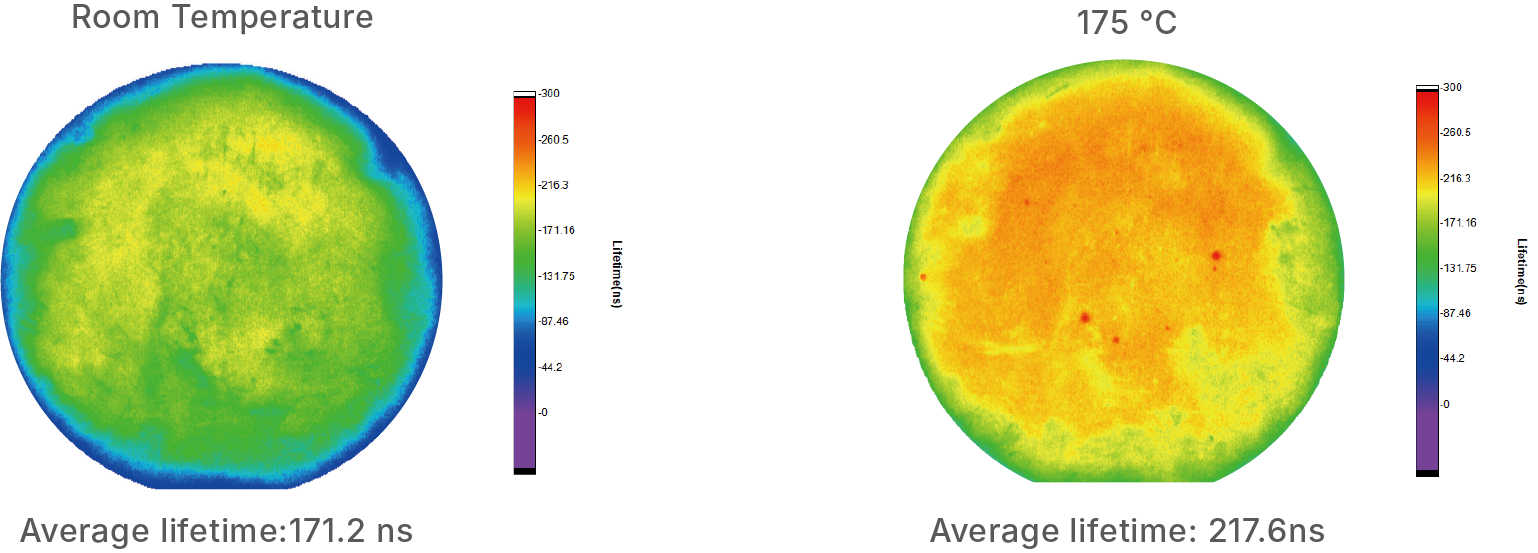
Switchable 355 nm and 266 nm excitation enables independent extraction and mapping of bulk minority carrier lifetime and surface recombination velocity. These tools support fully automated measurements, with optional nitrogen-purged or vacuum sample chambers to minimize environmental interference and preserve sample surface conditions. An optional temperature-control module spanning room temperature to 200°C enables temperature-dependent lifetime measurements for investigating carrier recombination mechanisms and trap-state characteristics.
These tools support both full-wafer mapping and localized microscopic imaging. In full-wafer mode, it achieves a spatial resolution of 100 μm to characterize minority carrier lifetime distributions and uniformity. It accommodates 6-, 8-, and 12-inch wafers, with measurement times of less than 10 minutes per 6-inch wafer. In microscopic mode, spatial resolution reaches 0.9 μm, enabling visualization of lifetime variations associated with threading dislocations and stacking faults. A temporal resolution of <2 ns enables characterization of both short-lifetime substrates and epitaxial layers.
Switchable 355 nm and 266 nm excitation enables independent extraction and mapping of bulk minority carrier lifetime and surface recombination velocity. These tools support fully automated measurements, with optional nitrogen-purged or vacuum sample chambers to minimize environmental interference and preserve sample surface conditions. An optional temperature-control module spanning room temperature to 200°C enables temperature-dependent lifetime measurements for investigating carrier recombination mechanisms and trap-state characteristics.
Inquire