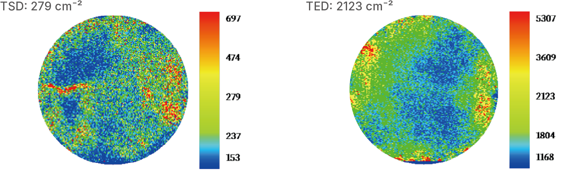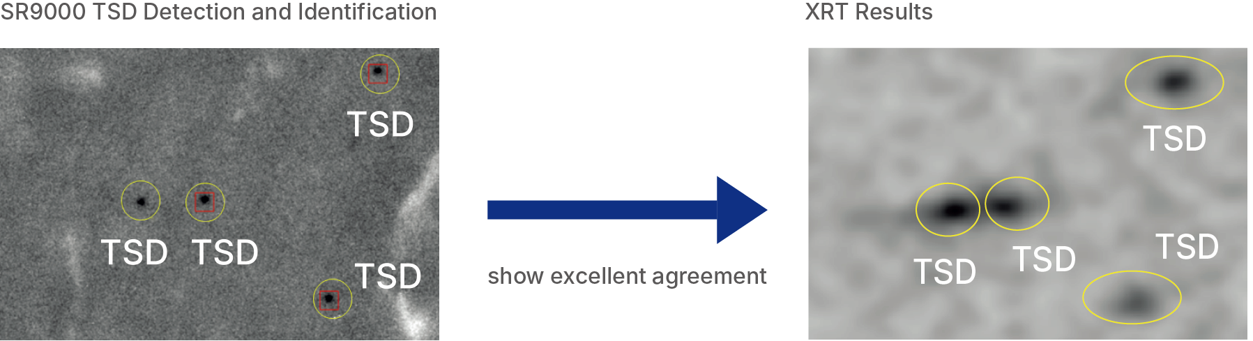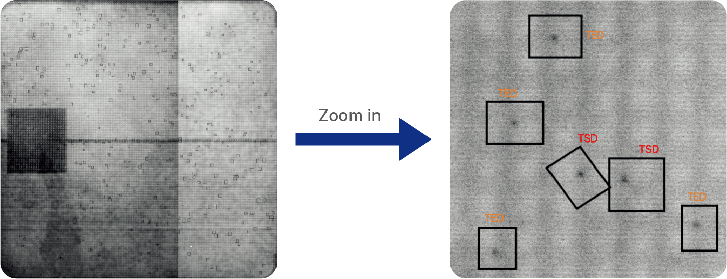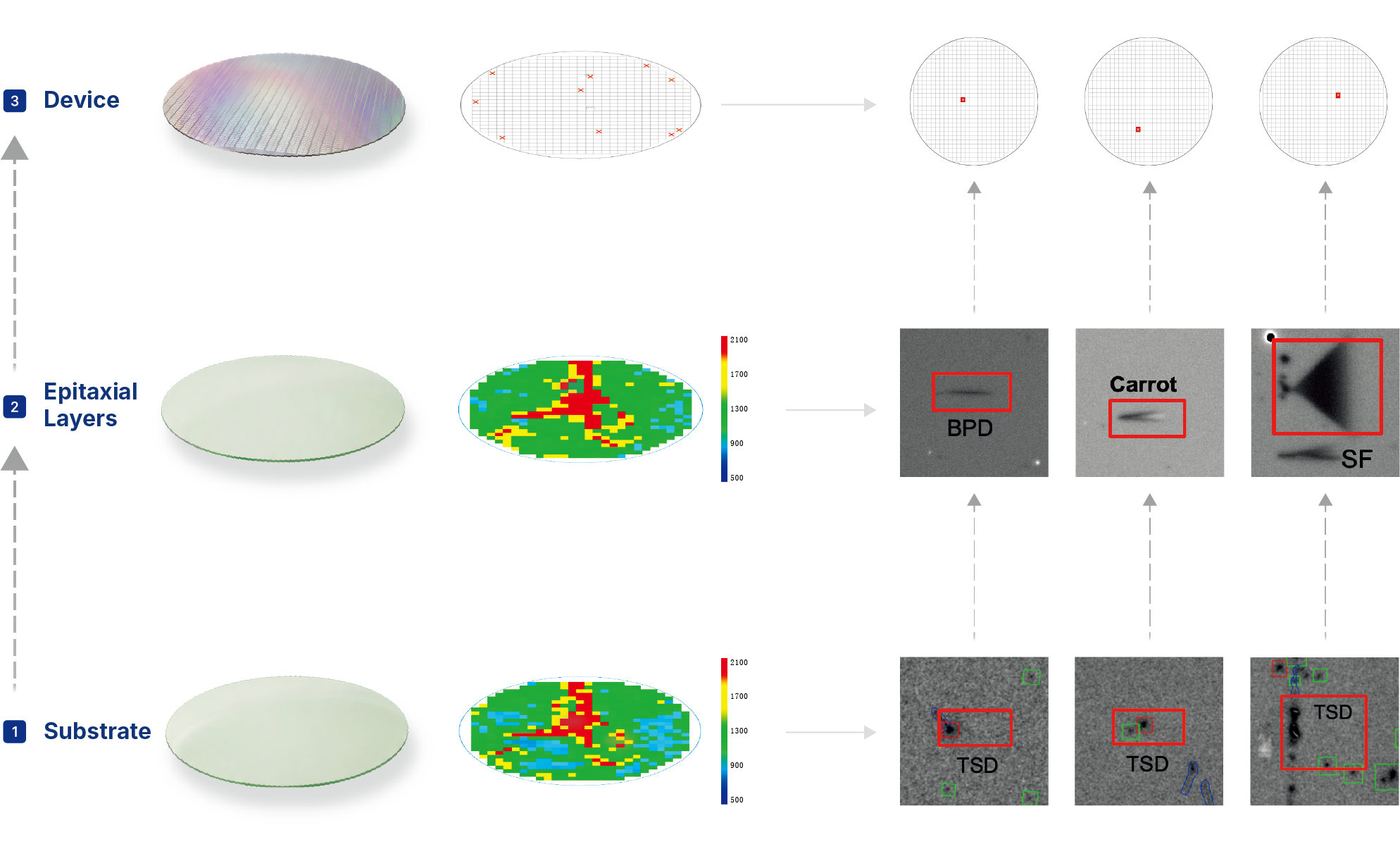

The SR-9000 Non-destructive Optical SiC Epitaxial Layer Defect Inspection System identifies, locates, and images dislocations and other defects in SiC epitaxial wafers and throughout device fabrication. It provides inspection data for material quality assessment, process optimization, and defect tracing.
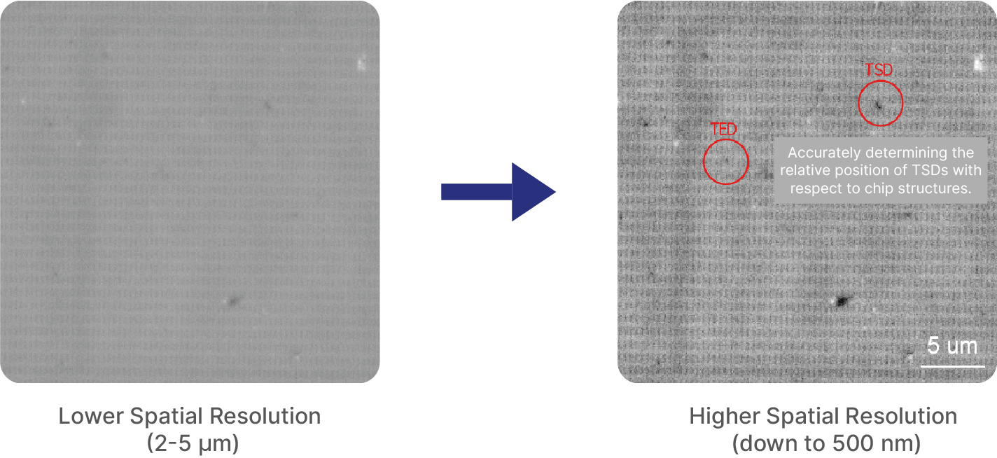
The system achieves a spatial resolution of 0.5 μm and supports full-wafer defect mapping. Detectable defects include threading screw dislocations (TSDs), threading edge dislocations (TEDs), basal plane dislocations (BPDs), stacking faults (SFs), triangle defects, and carrot defects. It accommodates 6-, 8-, and 12-inch wafers, with inspection throughputs of 4, 2, and 1 wafer per hour, respectively.
The system supports inspection of SiC epitaxial wafers, patterned device wafers, ion-implanted wafers, and SiC wafers and devices after metal layer removal. It enables dislocation inspection at key manufacturing stages, including the epitaxial layer, after gate oxide formation, and before top-metal evaporation. By combining high spatial resolution imaging with pattern deconvolution, it locates dislocations beneath patterned structures and helps trace defect evolution from substrates through epitaxial layers to devices, providing traceable inspection data to investigate defect origins and support yield improvement.
The system achieves a spatial resolution of 0.5 μm and supports full-wafer defect mapping. Detectable defects include threading screw dislocations (TSDs), threading edge dislocations (TEDs), basal plane dislocations (BPDs), stacking faults (SFs), triangle defects, and carrot defects. It accommodates 6-, 8-, and 12-inch wafers, with inspection throughputs of 4, 2, and 1 wafer per hour, respectively.
The system supports inspection of SiC epitaxial wafers, patterned device wafers, ion-implanted wafers, and SiC wafers and devices after metal layer removal. It enables dislocation inspection at key manufacturing stages, including the epitaxial layer, after gate oxide formation, and before top-metal evaporation. By combining high spatial resolution imaging with pattern deconvolution, it locates dislocations beneath patterned structures and helps trace defect evolution from substrates through epitaxial layers to devices, providing traceable inspection data to investigate defect origins and support yield improvement.
Inquire