4-5 wafers/hour (6"); 2-3 wafers/hour (8")
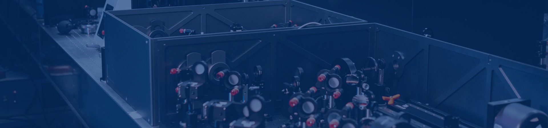

The SR-9000 is designed to address the defect inspection requirements of SiC epitaxial wafers and chips. It targets the current limitation in epitaxial wafer inspection, where precise quantification and spatial distribution of TSD and TED defects are difficult to obtain. Through high-precision detection, the system enables accurate identification and localization of TSD defects in SiC epitaxy and chips, providing critical support for further improvement of chip yield and performance.
The system supports defect inspection of SiC epitaxial wafers (pattern-free) and chips (patterned), enabling identification and classification of TSD, TED, and other defect types, including BPD, SF, SSF, BSF, triangular defects, and carrot defects. It achieves ultra-high localization accuracy, with TSD/TED localization accuracy <1 μm and chip structure localization accuracy <1 μm. The system throughput is 4–5 wafers per hour for 6-inch wafers and 2–3 wafers per hour for 8-inch wafers.
The system supports defect inspection of SiC epitaxial wafers (pattern-free) and chips (patterned), enabling identification and classification of TSD, TED, and other defect types, including BPD, SF, SSF, BSF, triangular defects, and carrot defects. It achieves ultra-high localization accuracy, with TSD/TED localization accuracy <1 μm and chip structure localization accuracy <1 μm. The system throughput is 4–5 wafers per hour for 6-inch wafers and 2–3 wafers per hour for 8-inch wafers.
Inquire

