| Availability: | |||||||||
|---|---|---|---|---|---|---|---|---|---|
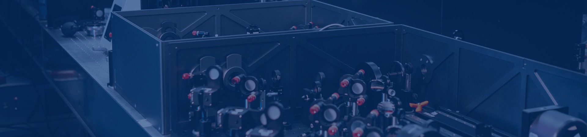
| The TAU‑9000 system employs pump‑probe‑based ultrafast transient spectroscopy imaging to achieve high temporal and spatial resolution characterization of wafer minority carrier lifetimes. Photogenerated carriers are excited by pump light, and their decay dynamics are measured through time-resolved imaging, enabling precise assessment of the effects of dislocations, point defects, and surface contamination on carrier lifetimes, thereby reflecting overall wafer quality. The system supports multiple wafer sizes (2″, 4″, 6″, 8″, 12″) and a range of materials including SiC, GaN, GaAs, InP, and Si, with a lifetime measurement range from <5 ns to several seconds, spatial resolution of 275 μm, and temporal resolution of 1–10 ns. A vacuum chamber prevents optical damage to the sample surface. Integrated AI algorithms enable quantitative defect density analysis and customized evaluation, allowing full-chain quality tracking from substrate, through epitaxy, to device. | |||||||||
TAU 9000
Utilizes ultra-fast transient optical spectroscopy imaging technology to achieve high temporal and spatial resolution
Incorporates a vacuum chamber to effectively prevent laser damage to the sample surface
Allows for separate detection of the wafer surface and bulk material by switching the excitation wavelength
Compatible with functions such as laser annealing and bipolar degradation detection
High-speed, high-throughput detection meets production line requirements
Overcoming Industry Challenges
The minority carrier lifetime of semiconductor wafers, such as SiC, is one of the key parameters indicating wafer quality. Measuring the minority carrier lifetime provides valuable insights into the point defect concentration and surface contamination by metal ions. Furthermore, as demand for high-voltage SiC devices continues to grow, the need for measuring the minority carrier lifetime of thick epitaxial wafers will also increase.
Specifications
| Inspection Time | 5 min/wafer (6", 8", and 12") |
Lifetime Inspection Window | <5 ns to seconds |
Spatial Resolution | 275 μm (6", 8", and 12") |
| Inspectable Samples | SiC、GaN、GaAs、InP、Si |
| Temporal Resolution | <1 ns to 10 ns |
| Compatible Sample Size | 2"、 4"、 6"、 8"、12" |
| Point defect concentration, surface contamination, carrier lifetime, and lattice quality evaluation | |
| Equipped with a vacuum chamber to prevent laser damage to wafer surfaces | |
Case Examples
Differing from the conventional μ-PCD technique, the TAU-9000 series uses transient spectroscopic full-wafer imaging to capture minority carrier lifetime data at high speed and with high spatial resolution, far exceeding traditional μ-PCD in key metrics like temporal resolution, spatial resolution, and throughput.
| TAU-9000 | Conventional μ-PCD | |
| Testing Principle | Pump-probe full-wafer single-shot imaging (High Efficiency) | Microwave Photoconductivity Decay (μ-PCD) Point-by-Point Scanning |
| Excitation Wavelength | 355 nm / 266 nm | 349 nm (Single Wavelength) |
| Temporal Resolution | < 5 ns (SiC) | > 30 ns |
| Spatial Resolution | 275 μm | >1mm |
| Scanning Time | < 5 min/wafer | ~90 min @ 0.5 mm Step Size |
Max Wafer Size | 12" | 8" |
