

The SL-9000 is a non-destructive optical inspection system for compound semiconductor substrates, designed primarily for indium phosphide (InP), with scalability to gallium arsenide (GaAs). Suitable for both conductive and semi-insulating substrates, the system images and maps threading dislocations and other lattice defects to support substrate quality assessment and process optimization.
Using defect-induced photoluminescence (PL) quenching, the SL-9000 reveals the microscopic features and spatial distribution of dislocations through variations in luminescence intensity, without destructive chemical etching. For InP substrates, the inspection depth is approximately 1–3 μm below the surface. Comparative studies on sulfur-doped and iron-doped InP samples show good correspondence between optically mapped dislocations and etch pit inspection results.
Equipped with an AI analysis system and compatible with bright-field and dark-field inspection, the SL-9000 also supports the assessment of surface defects, including scratches, particles, and contamination. Combining non-destructive inspection with efficient measurement, it supports compound semiconductor substrate research, manufacturing, and quality control.
Using defect-induced photoluminescence (PL) quenching, the SL-9000 reveals the microscopic features and spatial distribution of dislocations through variations in luminescence intensity, without destructive chemical etching. For InP substrates, the inspection depth is approximately 1–3 μm below the surface. Comparative studies on sulfur-doped and iron-doped InP samples show good correspondence between optically mapped dislocations and etch pit inspection results.
Equipped with an AI analysis system and compatible with bright-field and dark-field inspection, the SL-9000 also supports the assessment of surface defects, including scratches, particles, and contamination. Combining non-destructive inspection with efficient measurement, it supports compound semiconductor substrate research, manufacturing, and quality control.
PRODUCTS FEATURE
SPECIFICATIONS
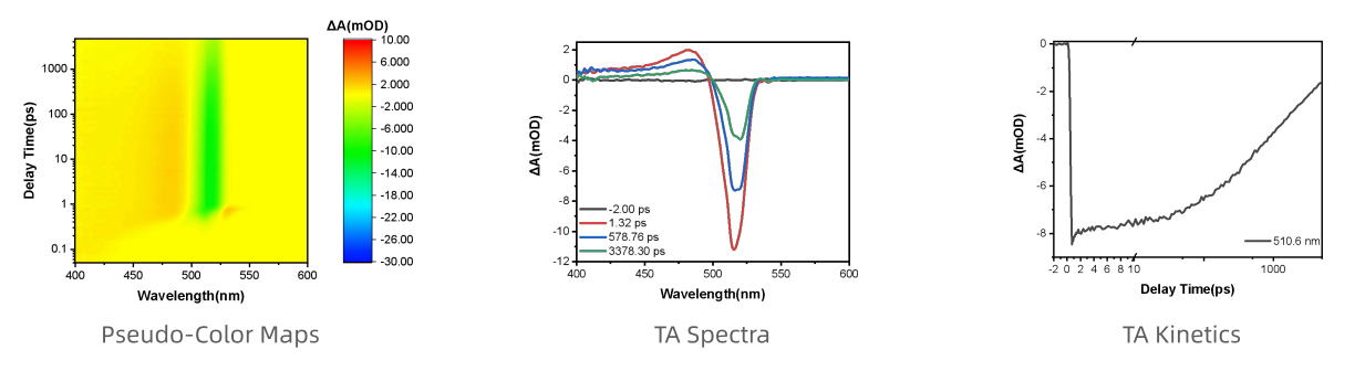
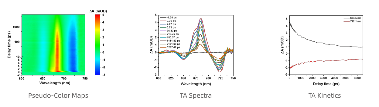
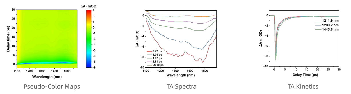
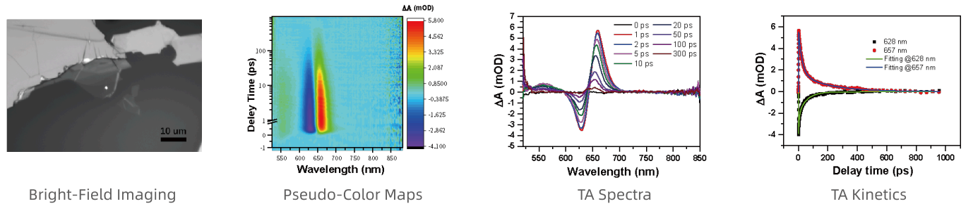
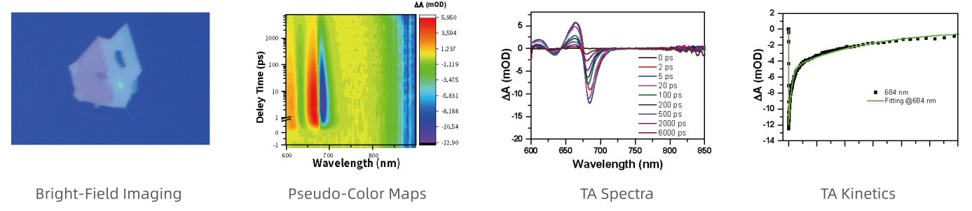
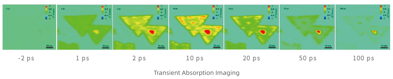
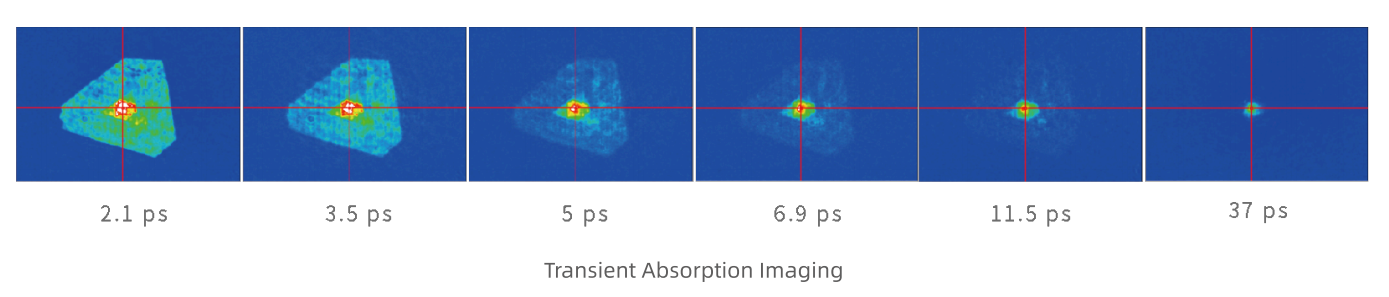
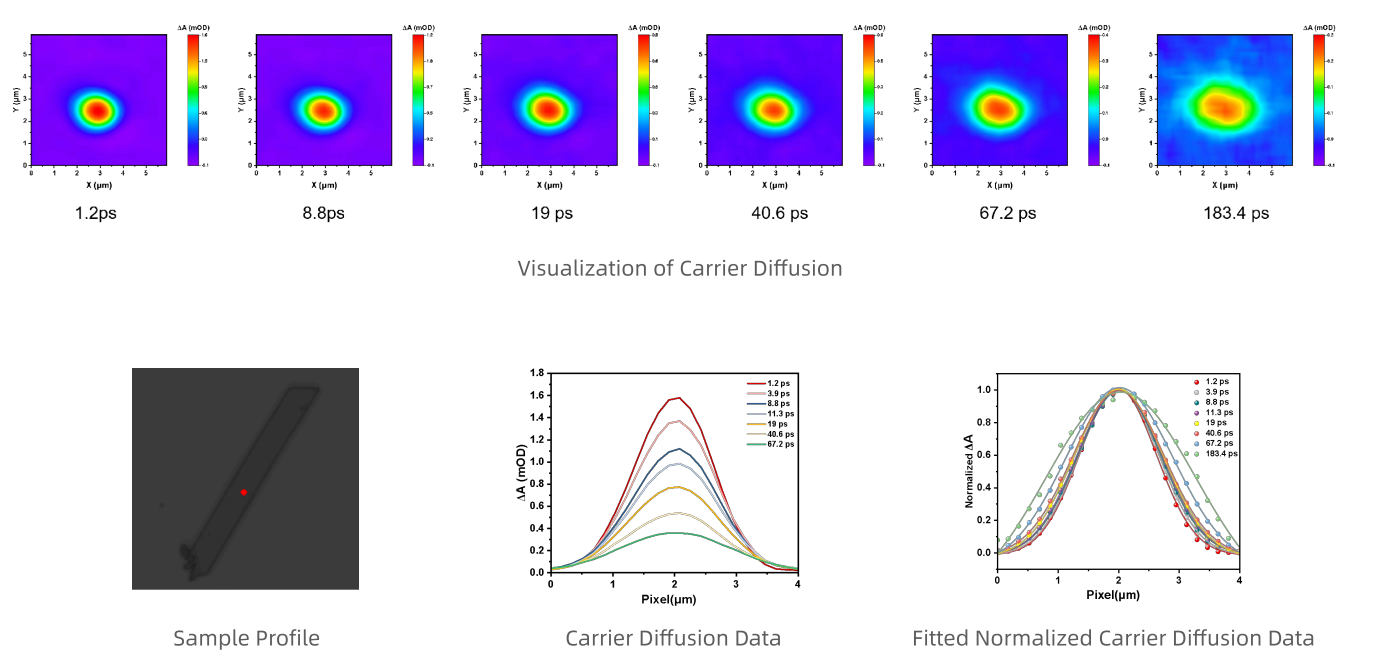
ULTRAFAST TRANSIENT ABSORPTION APPLICATION EXAMPLES
PUBLICATION
DOWNLOAD