| Availability: | |||||||||
|---|---|---|---|---|---|---|---|---|---|
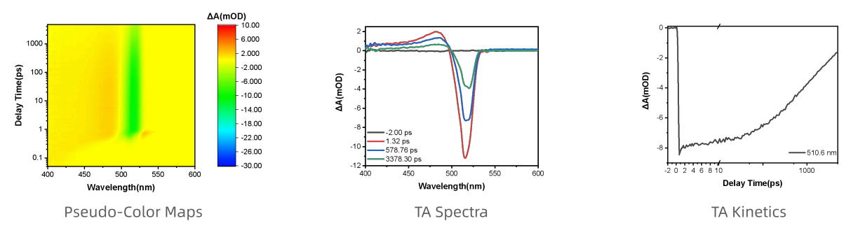
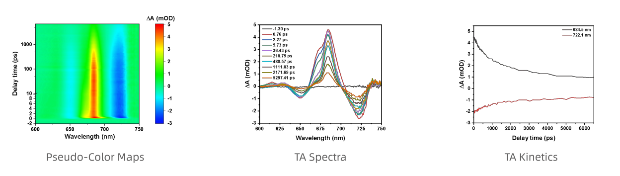
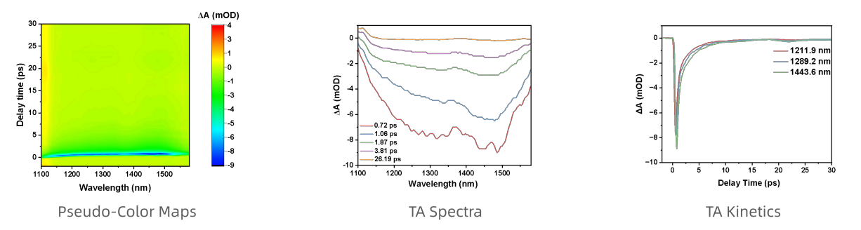
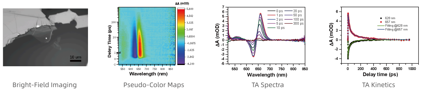
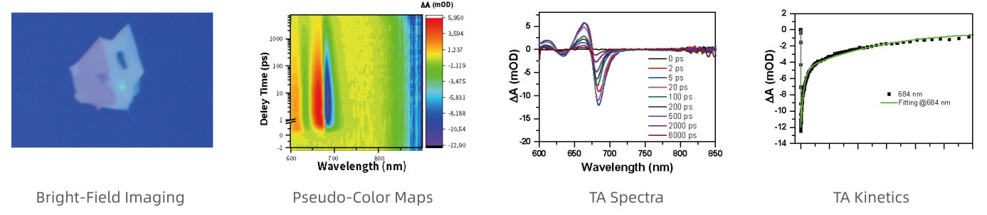
| The TA-AUTO and TA-MINI are transient absorption spectrometers designed to probe photo-induced electronic transitions and excited-state dynamics in various materials. TA-AUTO: Covers a broad spectral range from ultraviolet (UV) through visible and near-infrared (NIR) to mid-infrared (MIR). TA-MINI: Covers a broad spectral range from ultraviolet (UV) through visible. Supports time resolutions ranging from femtoseconds to microseconds. These systems can be integrated with a microscopy module to achieve high-spatial-resolution transient absorption spectroscopy. 
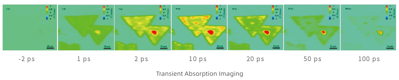
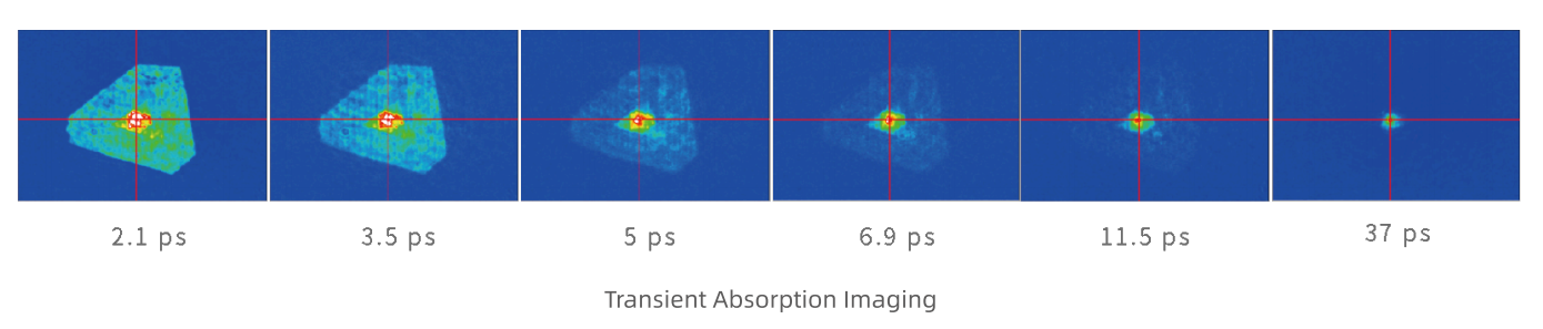
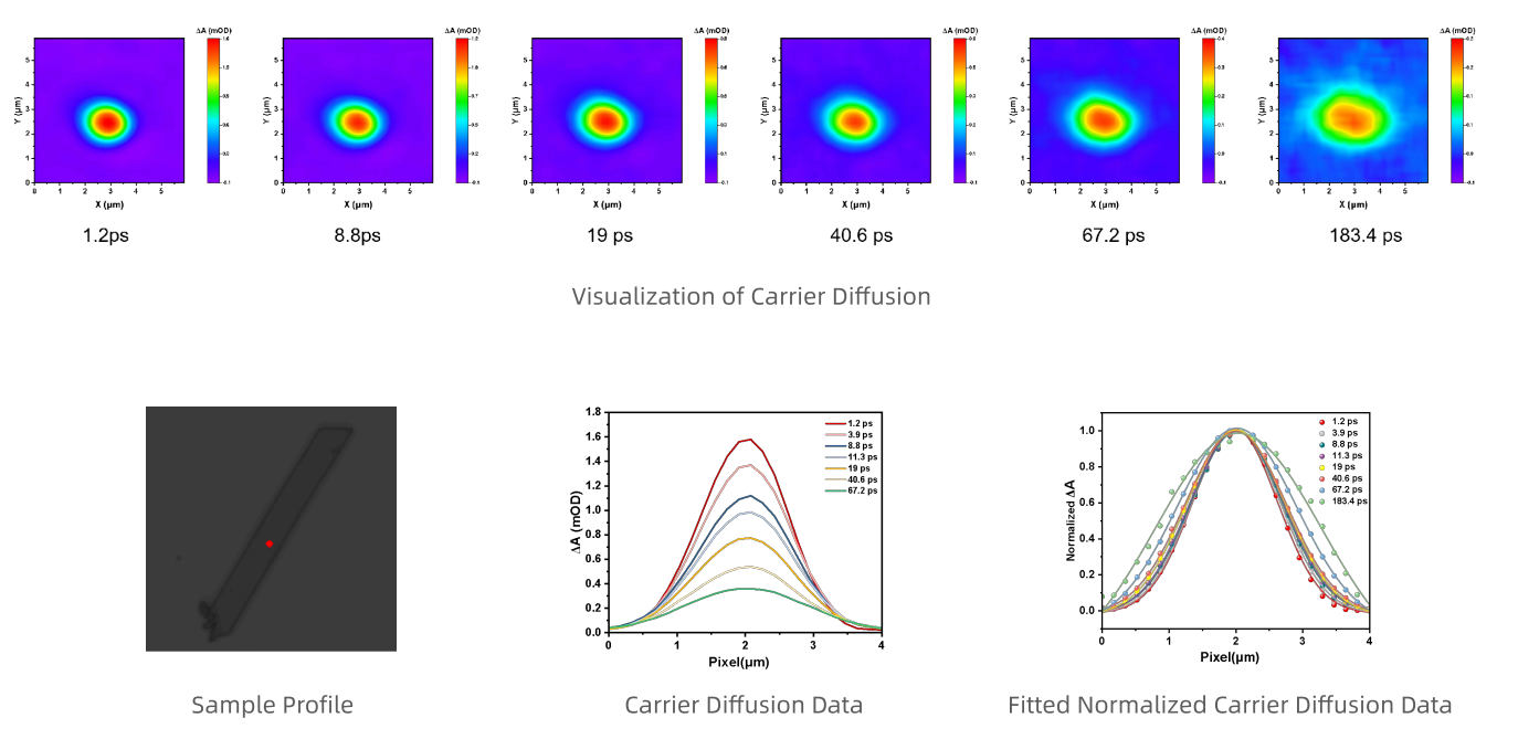
Additionally, these systems can incorporate a high-speed CMOS area camera to enable spatial defect mapping and the characterization of carrier diffusion and mobility. For high-repetition-rate laser sources, they can be further expanded with high-speed detectors to enhance detection sensitivity, achieving a detection limit as low as ≤10 -5 OD. | |||||||||
Products Features
Multi-mode Multi-range Detection: Equipped with transmission, reflection, and back-excitation modes. Detection spectrum covers UV to NIR bands, suitable for diverse samples including tetracene dimers and CdSe quantum dots, delivering excellent performance across UV-NIR ranges.
High Resolution: Temporal resolution ≤1.5×femtosecond laser pulse width; Spatial resolution ≤1μm (microscopic dynamics imaging module). Enables precise capture of transient processes, supporting carrier migration studies in photocatalysis and perovskite solar cells.
Automation & Intelligence: Fully automated optical path switching/calibration ensures operational stability. Integrated software for data acquisition/analysis improves experimental efficiency.
High Expandability: Modular design allows flexible configuration upgrades.
Specifications
Main
Time-Resolved Micro-Imaging Module
| Mode | Micro spectroscopy acquisition/wide-field TA imaging/Carrier diffusion imaging |
| Spatial resolution | ≤1 μm |
| Wavelength range | 400-800 nm |
| Carrier migration accuracy | 100 nm |
Nanosecond TA Upgrade Module
| Mode | Switchable transmission/Reflection | |
| Spectral Detection Range | 360-1700 nm | |
| Time window | ≤ 450 μs | |
| Time Resolution | 1 ns | |
| Maximum Detection Sensitivity | ≤ 0.1 mOD | |
| NS-SC Laser | Spectral Range | 350-1800 nm |
| Pulse Width | ~800 ps | |
| Repetition Rate | 2 KHz | |
| Power Stability | ±1% | |
| Total Average Optical Power | >5 mW | |
Electrical Excitation Module
| Maximum Voltage | ±5 V(±10 V) |
| Pulse Width | 6 ns - 999.99 s |
| Repetition Rate | 1 μHz - 80 MHz |
| Electrical Pulse Rise Time (0-5 V) | ≤5 ns (Default), optional ≤2 ns |
Ultrafast Transient Absorption Application Examples
UV Range Data
Sample Experiment
| Sample | Perovskite Thin Film |
| Excitation Wavelength | 405 nm |
| Probe Wavelength | UV |

Visible Range Data
Sample Experiment
| Sample | Ni-TPA |
| Excitation Wavelength | 370 nm |
| Probe Wavelength | Visible |

NIR Range Data
Sample Experiment
| Sample | Graphite |
| Excitation Wavelength | 495 nm |
| Probe Wavelength | NIR |

Micro Transmission TA
Sample Experiment
| Sample | Single layer WS2 (substrate: sapphire) |
| Excitation Wavelength | 515 nm |
| Probe Wavelength | Visible |

Micro Reflection TA
Sample Experiment
| Sample | Multilayer WS2 (substrate: Si) |
| Excitation Wavelength | 515 nm |
| Probe Wavelength | Visible |

Wide-field TA Imaging
Sample Experiment
| Sample | Monolayer WS2 |
| Excitation Wavelength | 515 nm |
| Probe Wavelength | 610 nm |

Near Infrared Imaging
Sample Experiment
| Sample | WS2 |
| Excitation Wavelength | 515 nm |
| Probe Wavelength | 900 nm |

Carrier Migration Data Diagram
Sample Experiment
| Sample | Perovskite-type Copper Fluoro-oxytitanate |
| Excitation Wavelength | 650 nm |
| Probe Wavelength | 800 nm |
